
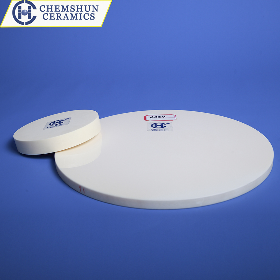
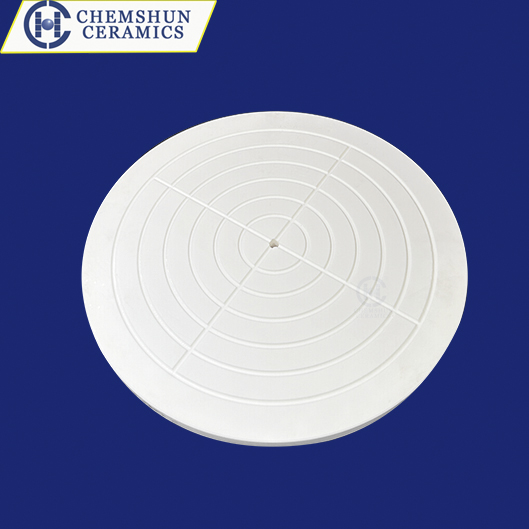
In semiconductor manufacturing, material selection is critical to process quality and product performance. 99.7% alumina ceramic wafer polishing plate, as a high-performance ceramic material, are widely used in the semiconductor industry due to their exceptional physical and chemical properties. This article explores the characteristics of 99.7% alumina ceramic wafer polishing plate and their vital role in semiconductor manufacturing.
1. Properties of 99.7% Alumina Ceramics
99.7% alumina ceramic is a high-purity material primarily composed of α-alumina (Al₂O₃). Its key properties include:
High Purity: The 99.7% alumina content ensures chemical stability, minimizing contamination risks in semiconductor processes.
High-Temperature Resistance: Stable at temperatures exceeding 1600°C, making it ideal for high-temperature processes such as diffusion, oxidation, and chemical vapor deposition (CVD).
Corrosion Resistance: Resists acids, alkalis, and corrosive gases, maintaining performance stability during etching and cleaning processes.
High Hardness & Wear Resistance: Exceptional hardness ensures minimal wear over prolonged use, extending service life.
Superior Insulation: Excellent electrical insulation properties suit environments requiring electrical isolation.
2. Applications in Semiconductor Manufacturing
99.7% alumina ceramic wafer polishing plate play a pivotal role in semiconductor manufacturing, including:
Wafer Handling: Used to secure and support wafers during lithography, etching, and thin-film deposition, ensuring stability in high-temperature and corrosive environments.
High-Temperature Processes: Withstands thermal shocks in diffusion furnaces and CVD equipment, maintaining dimensional stability to prevent wafer deformation.
Etching & Cleaning: Corrosion-resistant performance ensures durability in plasma etching and wet cleaning processes involving strong acids or alkalis.
Packaging & Testing: Provides a stable platform for chip packaging and testing, ensuring process precision.
3. Advantages and Challenges
The advantages of 99.7% alumina ceramic wafer polishing plate lie in their high purity, thermal stability, and corrosion resistance, meeting the stringent demands of semiconductor manufacturing. However, challenges include complex manufacturing processes, high costs, and stringent requirements for surface flatness and dimensional accuracy, posing technical hurdles for production.
4. Future Outlook
As semiconductor technology advances, the performance requirements for ceramic trays will continue to rise. Future developments may focus on material modifications and optimized manufacturing processes to enhance thermal conductivity, mechanical strength, and cost-effectiveness, addressing the needs of next-generation semiconductor fabrication.
Post time: Mar-07-2025